

Basics of LCD Flicker
What is Flicker
01
TFT-LCD uses voltage changes to control the strength of the electric field in the liquid crystal box, changes the alignment direction of the liquid crystal molecules, and achieves control over whether light is transmitted. When the LCD displays the screen, the picture often appears, and this phenomenon is called "Flicker".
Why can the human eye observe Flicker
02
When the human eye observes a scene, it takes a short period of time to transmit the light signal to the brain. When the light effect is over, the visual image will not disappear immediately. This residual vision is called "post-image", which is called "visual temporary retention", also called "afterglow effect". Due to the afterglow effect, the human eye needs to feel the motion picture, and the picture update frequency remains at least 16 ~ 24Hz. However, in fact, the picture brightness difference can still be felt at the 30Hz picture update frequency, and the intuitive feeling is to see the picture flicker. Therefore, to obtain better picture quality, the higher the picture update frequency, the better.
Why do people observe the Flicker phenomenon when displaying a LCD monitor? It is because the brightness (gray level) of the front and rear display screens are inconsistent, and the brightness is because the light transmission of the LCD box is different, and the light transmission is determined by the degree of deflection of the liquid crystal molecules.
The mechanism of generation of Flicker
03
The LCD controls the liquid crystal standing angle by the voltage magnitude to control the brightness, and the liquid crystal is driven in an AC mode. As shown in the figure below, if the Vcom value is not adjusted well, because the existence of ΔVp is equivalent to applying a DC voltage in the liquid crystal layer, Vp+ ≠ Vp-, resulting in differences in brightness of positive and negative frames, resulting in flickering and other phenomena, which shortens the life of the liquid crystal; therefore, it is necessary to offset the sudden voltage ΔVp. In order to offset the part of the sudden voltage ΔVp, the common voltage Vcom can be turned into a variable (can be adjusted), which can effectively solve the problem of Flicker.

An important factor that determines the quality of the TFT switch is the parasitic capacitance Cgs between the TFT gate metal and the source metal. Generally, the side where the TFT is connected to the pixel electrode is set as the source. Since the switch of the TFT is close to a transient, when the gate voltage Vgs drops instantly from the high level VGH to the low level VGL, the change amount of Vgs ΔVgs is combined on the pixel electrode by the TFT parasitic capacitor Cgs, causing the pixel voltage Vp to jump, and the jump is ΔVp. Due to the existence of ΔVp, the pixel voltage becomes (Vp-ΔVp).
Flicker's evaluation method
04
When positive and negative frame transformations under a conventional picture, adjacent pixels compensate each other, making the flicker flicker of the conventional picture unobservable. When the positive and negative frames change in the flicker screen state, the Flicker flicker can only be observed due to the deviation of the brightness of the positive and negative frame pixels. Below are two common Flicker evaluation methods in the industry.
There are generally two types of flicker testing methods in the VESA (Video Electronics Standards Association) standard: JEITA test method and FMA test method.
The JEITA test method is to adjust the refresh frequency of the display to the frequency when it is in operation, and uses a spectrum meter and photoelectric conversion device to test the change curve of brightness over time within a frame. Through fast Fourier transformation, it is converted into the change curve of brightness over frequency F(w). Next, take F(ω) at the same frequency as the sample being tested, if you take F60Hz and F0Hz at DC, then take the logarithm of F(ω)/F0Hz, the result is the flicker value, and the formula is expressed as:

The test conditions of the FMA (Flicker Modulation Amplitude, FMA) test method are the same as that of the JEITA method. The brightness is converted into amplitude modulated electrical signal through a photoelectric converter, and the maximum value of Vmax and minimum value of Vmin are read. It is qualitatively believed that (VmaX-Vmin) is an AC component and (Vmx+Vmin)/2 is a DC component. Then the expression of MaX flashing is:

The impact of Vcom on Flicker
05
The optimal flicker of the products in the white mode gradually decreases as the gray level increases, while the optimal flicker of the black mode products gradually decreases, but the corresponding Vcom gradually increases.
The ΔVp, the normal white mode product, gradually increases as the gray scale increases (Vcom negative shift), thereby causing the positive and negative brightness difference to increase, but the average brightness of the picture also shows an increase trend as the gray scale increases (main factors), which leads to the reduction of the optimal flicker; while the ΔVp, the gray scale of the normal black mode product, gradually decreases (Vcom positive shift), thus causing the positive and negative brightness difference to gradually decrease, and since the average brightness of the picture also shows an increase trend, the optimal flicker gradually decreases.

The impact of VGH on Flicker
06
In the experiment, the VGH voltage was externally connected to the DC power supply, and VGL and Vcom remained unchanged. The flicker values under different VGH voltages in the normal white mode and the normal black mode products were tested respectively. The results are shown in the figure below, indicating that VGH has a significant impact on flicker. The reasons for analysis are:
In the first stage, when VGH is low, on the one hand, ΔVp increases with the increase of VGH. On the other hand, when VGH is low, the pixels are not fully filled, and the brightness difference of positive and negative frames is large (main factor). As VGH increases, the pixels gradually fill, and the brightness difference of positive and negative frames decreases. In this stage, flicker decreases with the increase of VGH;
In the second stage, VGH increases to a certain extent and the pixels are fully filled. At this time, ΔVp increases with the increase of VG, which causes the brightness difference of positive and negative frames to increase, that is, the flicker increases.
The VGH voltage is different from the two modes of products, and the optimal flickering and corresponding Vcom relationship. The experimental results shown in the figure below show that VGH increases and the optimal flicker is almost unchanged, but the corresponding Vcom gradually decreases. Therefore, when the VGH voltage changes, the flickering can be adjusted to achieve the best flickering.
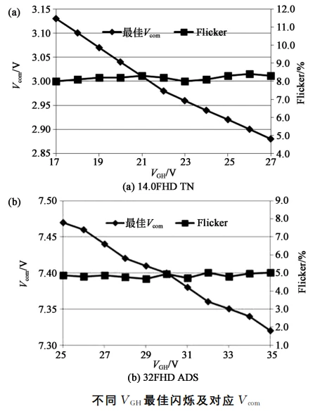
The impact of VGL on Flicker
07
In the experiment, the VGL voltage was externally connected to the DC power supply, and VGH and Vcom remained unchanged. The flicker values under different VGL voltages in the normal white mode and the normal black mode products were tested respectively. The results are shown in the figure below, indicating that VGL has a significant impact on flicker. The reasons for analysis are:
In the first stage, when VGL gradually decreases from -2 V to the lowest point (about -8 V), although ΔVp gradually increases, the Ioff of the TFT gradually decreases (main factor), and the pixel voltage has better retention characteristics, which causes the brightness difference of positive and negative frames to gradually decrease, that is, flicker gradually decreases;
In the second stage, VGL continues to decrease, and the Ioff of ΔVp and TFT gradually increases. The combination of the two causes the brightness difference between positive and negative frames to gradually increase, that is, the flicker gradually increases.

What is Flicker drift
08
When there is a DC bias electric field in the LCD, the bias electric field attracts ions, causing a built-in electric field to be generated near the electrode. This built-in electric field continues to strengthen until the DC bias electric field compensation is completed. The interaction effect of this built-in electric field and DC biased electric field causes the Flicker to drift.
Effect of pixel polarity reversal on Flicker
09
The phenomenon of Frame inversion polarity transformation method is obvious
The phenomenon of Flicker inversion polarity transformation method is not obvious
The phenomenon of Flicker in the Column inversion polarity transformation method is not obvious
Dot inversion polarity transformation method Flicker is almost no phenomenon
Usually we optimize the Flicker phenomenon by adjusting the Vcom voltage and selecting the polarity inversion method.


