

Hey everyone, if you buy and sell TFT LCD modules for a living, you've probably come across the term "Array process" more times than you can count. But let's be honest - most people don't really know what happens during this stage or why it matters so much to the final product quality and cost. I've spent more than ten years working in large panel factories, and I can tell you from experience that the TFT LCD Array process is where everything starts. Get this part right, and you have a much better chance of stable yields and happy customers. Get it wrong, and you'll be dealing with defects, returns, and price complaints later.
In this article, I'm going to explain the TFT LCD Array process in plain language the way I would explain it to a new distributor partner. No fancy theory, just the real stuff that affects your daily sourcing decisions.
What Exactly Is the TFT LCD Array Process?
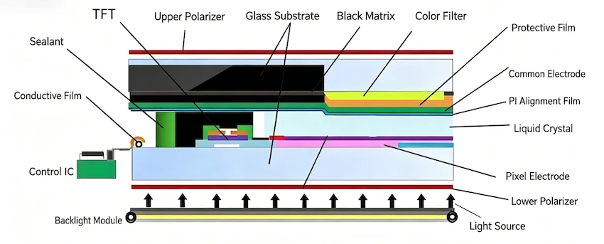
The Array process is the very first major stage in making a TFT-LCD panel. This is where we build the thin-film transistors directly onto a large sheet of glass. These tiny transistors act as switches that control each pixel - turning them on and off to create the image you see on the screen.

A full TFT-LCD panel has three main front-end parts: the Array (TFT glass), the Color Filter glass, and the Cell process where they get joined together with liquid crystal. The Array stage is by far the most expensive and precise because it's basically semiconductor manufacturing, but done on glass instead of silicon wafers.
Most standard a-Si TFT LCDs these days use somewhere between 5 to 7 masks. The most common design is called bottom-gate structure, where the gate electrode sits underneath the semiconductor layer.
Walking Through a Typical 5-Mask Array Process
Let me take you through a standard 5-Mask flow for a basic TN mode panel. This is still very widely used for cost-sensitive products.
Mask 1: Gate Lines and Electrodes We start with perfectly clean glass sheets. Then we sputter metal layers (usually some kind of aluminum or copper stack) onto the glass. After coating photoresist, exposing it with UV light through a mask, developing, and wet etching, we end up with the horizontal scan lines and gate electrodes. This is often called M1 layer.
Mask 2: Gate Insulator and Semiconductor Island Next we use CVD equipment to deposit silicon nitride as the insulator, followed by amorphous silicon as the semiconductor material. We pattern this to create small "islands" where each transistor will sit. This step is critical for the switching performance of the TFT.
Mask 3: Source, Drain, and Data Lines We deposit another metal layer and pattern the source and drain electrodes plus the vertical data lines. We also etch the channel area here. At this point, the basic transistor structure is pretty much complete.
Mask 4: Passivation Layer and Contact Holes We add a protective silicon nitride layer on top and open small contact holes (vias) so the pixel electrode can connect electrically to the transistor.
Mask 5: Pixel ITO Electrode Finally, we deposit transparent ITO and pattern the pixel electrodes. This is the layer that will actually apply voltage to the liquid crystals later.
For IPS or FFS panels that need better viewing angles, we usually add a sixth mask for the common electrode (COM ITO).
Every single mask follows roughly the same cycle: deposit the film, coat photoresist, expose, develop, etch (wet for metals, dry for non-metals), and strip the photoresist. The alignment between layers has to be extremely precise - even a tiny shift can cause line defects or dead pixels.

Key Materials Used in the TFT LCD Array Process
Glass Substrate Everything starts with special alkali-free glass. Normal glass that contains sodium or potassium just doesn't work here. Those alkali ions can move around under voltage and mess up the TFT performance, causing flickering, image sticking, or uneven brightness. The glass also needs excellent light transmission and must handle high temperatures without warping.
Metal Layers for Gate and Data Lines We rarely use pure aluminum or copper anymore. Instead, we use composite stacks like Mo/Al/Mo or Ti/Cu/Ti.
Aluminum has been the traditional choice because it's cheaper, but copper is becoming more popular. Copper has much lower resistance, which lets us make narrower lines, increase the aperture ratio, improve light transmission, and reduce overall power consumption.
The barrier metals (molybdenum, titanium, niobium) are there to improve adhesion to the glass and stop metal atoms from diffusing into the silicon layer, which would destroy the transistor's performance.
Amorphous Silicon (a-Si) This is the semiconductor material that forms the channel of the transistor. It's mature, relatively cheap, and easy to produce, but its electron mobility is low. That's why a-Si is great for medium and low resolution panels but not ideal for very high PPI screens.
We also add a heavily doped N+ a-Si layer to create good ohmic contact between the silicon and the metal electrodes, reducing resistance and improving reliability.
Silicon Nitride (SiNx) Used as both the gate insulator and the final passivation layer. It protects the transistor from moisture and ions while helping create a stable interface with the amorphous silicon.
ITO Transparent Conductor Indium Tin Oxide is what we use for the pixel electrodes. It needs to be both conductive and highly transparent. Key specs include low sheet resistance and transmittance above 80%. One thing many buyers don't realize is that ITO is quite sensitive to moisture. If the panels aren't stored properly, the ITO can degrade and cause problems later in production.
Real Challenges I've Seen in Production
In real factories, keeping particles under control during the TFT LCD Array process is an endless battle. Even microscopic dust can create visible defects. I remember one project for industrial 10.1-inch panels where the initial Array yield was only around 74%. After months of fine-tuning the cleaning process and deposition uniformity, we pushed it above 92%. That improvement cut costs noticeably and made the wholesaler much happier with repeat orders.
Practical Tips for Wholesalers and Distributors
When you're talking to suppliers, here are some useful questions to ask about their TFT LCD Array process:
- What mask count are they using for this particular product?
- What's the current yield at the Array stage?
- Have they switched to copper electrodes for lower power designs?
- How do they control particle contamination?
Suppliers who handle the full flow from Array through final LCM module usually have better overall consistency.
The industry is slowly moving toward newer oxide TFT materials for higher performance, but good old a-Si still dominates a large portion of the market because of its cost advantage and mature production.
Final Thought
If you're a wholesaler or distributor tired of dealing with inconsistent quality or suppliers who can't explain their process clearly, it might be time to find a better partner.


At Minghua, we focus on custom LCD business and have strong capabilities across the entire production chain, including deep understanding of the TFT LCD Array process. We work closely with distributors and wholesalers, offering everything from standard modules in volume to fully custom TFT LCD solutions for demanding applications.
Whether you need reliable supply, technical support, or help optimizing cost and performance for your customers, we're here to help. Feel free to reach out and tell me about your current projects - I'd be glad to see how we can support your business with better LCD solutions.


